Ruggedizing Electronics: Best Practices for Bullet-proof Devices
As electronic devices continue to permeate various industries, from aerospace and automotive to military and industrial applications, the need for electronics to withstand harsh conditions becomes paramount. Printed circuit boards (PCBs), which form the backbone of virtually all electronic devices, determine the reliability and efficiency of electronic systems in mission-critical applications.
Ruggedizing PCBs is a critical engineering endeavor aimed at enhancing their resilience in challenging environments. It involves a series of design and manufacturing techniques focused on fortifying PCBs against extreme temperatures, moisture, vibration, and mechanical shock. The challenge for PCB manufacturers is to identify ruggedizing methods that are well-suited to each application.
This article delves into the principles, methods, and benefits of ruggedizing PCBs. The article discusses some case studies highlighting the significance of ruggedization in modern engineering applications. A comparison-based analysis identifies pros and cons of different techniques. Finally, the article concludes by highlighting some products from Chemtronics & Techspray to aid electronics manufacturers in the ruggedization process.
Underfill
Mechanical strength in PCBs is one of the most vital factors for ensuring their longevity and reliability. It safeguards against physical stresses like bending, vibration, and shock during handling and transportation. Without adequate mechanical strength, PCBs may suffer from solder joint failures, component displacement, or even structural damage leading to electrical faults and system malfunctions.
A robustly-designed PCB with sufficient mechanical strength ensures stability and resilience in diverse operational environments, enhancing overall product quality.
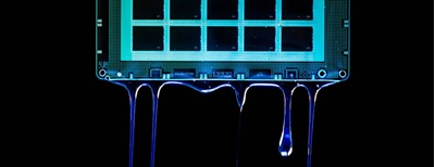
Underfill is one of the methods of PCB ruggedization employed to shield solder joints and balls linking a chip to a printed circuit board (PCB). Particularly in fine-pitch ball grid array (FBGA) packages (widely used in portable electronic devices), underfill is typically applied at the Surface Mount Technology (SMT) stage to bolster the mechanical integrity of the product [1].
The conventional underfill procedure employs the capillary effect to guide resin into the substrate space underneath the chip, followed by curing the resin by heat to strengthen solder joints. Another approach entails immersing the solder ball directly into the encapsulant of the solder joint. It traverses the reflow oven to create solder joints and aid in the solidification of the encapsulant.
A case study [1] analyzes the drop performance of FBGA packages with the help of finite element simulations (FEM). The experiment applies a 1500G load with a 0.5ms half-sine shock pulse, adhering to the JEDEC standard. The most common failure mode during drop impacts is the detachment of solder balls and copper pads. The outcome of the study indicates that drop performance in a solder joint structure receiving full reinforcement via the traditional underfill process surpasses a partially reinforced structure formed through the solder joint encapsulant underfill method [1].
Figure 1 and Figure 2 demonstrates this result. The stress value at solder joints with solder joint encapsulant underfill process is 35 MPa while it is 17 MPa with an epoxy underfill process. Moreover, without an underfill, a dropped PCB may cause relative motion between the components and PCB, then malfunctioning. Besides ensuring mechanical strength, underfill also reduces thermal stress in solder balls between the silicon die and substrate.
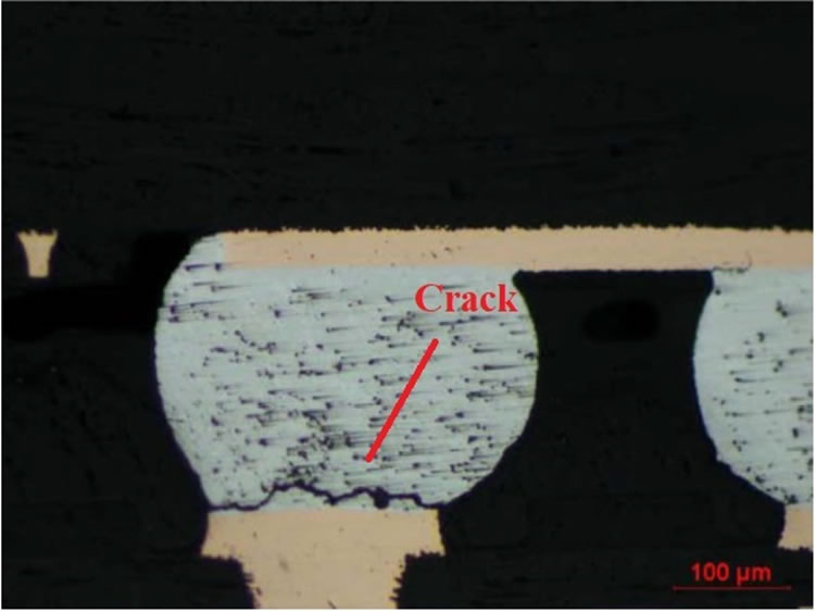
Figure 1: Cross-sectional view of FBGA package with solder joint encapsulant adhesive [1]
Edge/Corner Bonding
Edge bonding, a low cost variant of underfilling, involves affixing only the edges/corners of the component to the printed circuit board with the help of a viscous adhesive. In edge bonding, adhesive does not flow to the solder balls. Edge-bonded components offer the advantage of being more straightforward to replace and inspect compared to their underfilled counterparts.
In fracture tests conducted on BGA-PCB specimens with underfill and edge-bonding, it was observed that, when the adhesive fillet size and shape were consistent, edge-bonding demonstrated an efficacy equal to that of underfilling in enhancing the bending performance of a PCB assembly with BGA components [2].
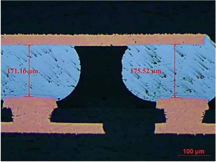
Figure 2: Cross-sectional view of FBGA package with generic epoxy underfill [1]
EMI Shielding
With the widespread adoption of 5G wireless technology and the potential it holds for Internet of Things (IoT) and critical communications, there is a growing imperative to protect electronics from Electromagnetic Interference (EMI). The prevailing approach to implement EMI shielding particularly in molded component packages has been the deposition of multiple metal (copper) layers through sputtering. This technique allows for the precise application of ultra-thin coatings of pure metal or metal alloys on package surfaces, typically within the 1-7μm thickness range [3]. However, the heavy initial investment required in sputtering equipment hinders its use in large-scale electronics manufacturing. As compared to sputtering, the spray-coating process for EMI shielding is scalable. For high-volume manufacturing conditions and employing an optimized spray process, the cost per unit for spray coating is lower than for sputtering [3].
Another commonly used method for EMI shielding is the use of metal enclosures. However, electromagnetic leakage primarily arises at the junction where the upper and lower shells of metal enclosures meet. To overcome this, a conductive adhesive is applied to secure the connection between these two shells. One case study [4] discusses varying thickness (1 mm, 2 mm, and 3 mm) and conductivity levels (0.2 S/m, 2 S/m, 20 S/m, and 200 S/m) of conductive adhesive to assess the impact on shielding effectiveness.
The results of the study are presented in Figure 3 and Figure 4. These results clearly portray a direct relationship. The thickness or conductivity (or both factors) can enhance the shielding effectiveness of the metal enclosure [4]. The CircuitWorks Conductive Epoxy offers outstanding electrical conductivity, forming a robust and high-strength bond. A volume resistivity of less than 0.001 ohm-cm implies an electrical conductivity of 105 S/m. Its mixed composition allows for a convenient five-minute work window and rapid curing. CircuitWorks® Conductive Epoxy bonds aggressively to a wide variety of materials.
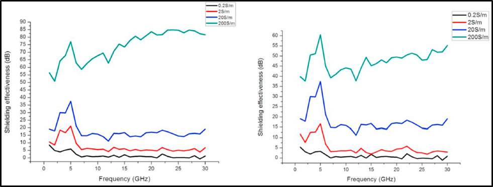
Figure 3: Shielding effectiveness with fixed thickness (2mm left and 1mm right) and varying conductivity [4]
The metal enclosures contain openings, or slits, designed for ventilation, communication, and power supply. When the enclosure interacts with an incident field, induced currents emerge on its surface. These induced electrical currents work to counteract or diminish the radiation intensity of the incident field. The presence of an opening on the enclosure's body disrupts the induced currents, leading to a reduced shielding effectiveness. To address this issue, the slits must be parallel to the direction of the induced current flow [5].
Figure 5 provides the visual explanation. If the shielding enclosure features a large slit, dividing it into several appropriately-sized smaller slits can substantially enhance shielding effectiveness, as it facilitates improved induced-current flows. If the enclosure necessitates sizable slits for ventilation purposes, it is advisable to utilize waveguides designed in a beehive-like configuration [5].
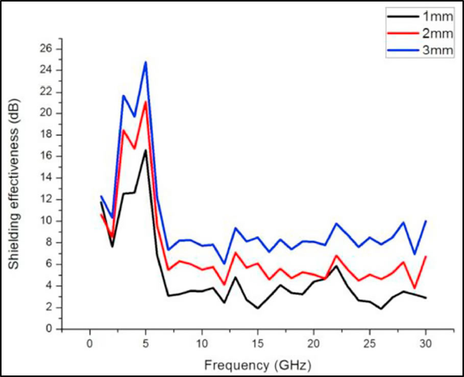
Figure 4: Shielding effectiveness with conductivity 2 S/m and varying thickness [4]
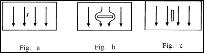
Figure 5: Induced currents with different slit configurations [5]
Potting and Low Pressure Molding
Potting and low-pressure molding are encapsulation methods used in electronics to protect components from extreme temperatures, moisture, dirt, and vibrations. Potting involves placing the electronic component in a mold, and then pouring a liquid resin (usually an epoxy) around it. This resin then cures and hardens around the component.
Low-pressure molding on the other hand, uses specialized equipment to melt a thermoplastic material and inject it around the component. The material solidifies upon cooling. Potting can have longer cycle times because of the longer curing process. Low-pressure molding is less expensive and usually has shorter cycle times since it relies on melting and cooling, which is faster than curing.
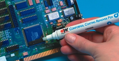
Conformal coating
Conformal coatings are thin, electrically-insulating films applied to assembled PCBs after soldering & cleaning steps. Conformal coatings shield PCBs from corrosive gases, dust, and humidity. But they also mitigate the risk of short circuits stemming from the expansion of tin whiskers.
Table 1 summarizes the traditional five types of coatings along with their pros and cons. Figure 6 helps manufacturers to select the coating best suited to their application.
It is important to emphasize that while conformal coatings offer moisture resistance, they do not provide waterproofing. Therefore, they are not suitable for applications exposed to prolonged wet conditions. In such cases, it is advisable to employ a waterproof enclosure, with the boards coated conformally inside.
Conformal coating serves well in safeguarding against issues like condensation, especially when transitioning from a cold environment to a warm, humid one. Thoroughly cleaning the PCBA is mandatory to ensure proper coating adhesion [6]. To delineate the areas designated for coating application and those meant to remain uncoated, the use of masking techniques is typically required. This may involve the application of masking tapes or adhesive circles to safeguard flat surfaces and openings from receiving the coating.
Latex masking material is employed to effectively mask surfaces with irregular shapes or contours. Typically, a coarse substrate with elevated surface energy will demonstrate superior wetting and coating adhesion compared to a smooth substrate with lower surface energy [6].
|
Type |
Advantages |
Disadvantages |
|
Acrylic |
Easy to apply and remove. |
Less environmentally friendly. Not suitable for low-temperature applications. |
|
Urethane |
Low outgassing characteristics – preferable for space applications. |
Difficulty of removal. |
|
Epoxy |
Provides excellent mechanical support to onboard components. |
Difficulty of reworking. |
|
Silicone |
Works over a wide temperature range. Excellent thermal endurance – best suitable to power electronics. |
Improper handling can cause contamination, resulting in adhesion issues on other PCBAs. |
|
Para-xylylene |
Greatest dielectrics strength, lowest outgassing, lowest weight. Exceptional resistance to moisture. |
Its thinness makes reworking very difficult. |
Table 1: Conformal coating types with pros and cons [6]
Moisture Prevention
Amongst all environmental factors, moisture is the primary culprit behind a significant portion of electronic failures, posing a major concern for electronics manufacturers. Our detailed article, The Essential Guide to Waterproofing Electronics, highlights methods and products to prevent electronics from moisture intrusion.
Figure 6: Conformal coatings rated from good to bad (1 to 5) [6]
Thermal Management
The process of ruggedizing PCBs starts from the design process. In this context, the effectiveness of thermal vias has been extensively researched, both in academia and the industry, particularly in compact electronic devices where incorporating large radiators is impossible. Using filled thermal vias is a prevalent technique in PCB design. Greater plating thickness enhances the thermal resistance of these vias.
he case study [7] explores the patterns of thermal vias for greatest heat transfer or better thermal behavior. The experiment involves designing a PCB assembly in SolidWorks by mounting a DPAK component to PCB. Three types of vias arrangements under consideration are shown in Figure 7.
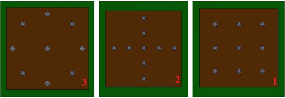
Figure 7: Via distribution patterns under DPAK component [7]
The simulated vias have an outer diameter of 0.3 mm and an inner diameter of 0.2 mm. The cooling method for the simulation relies on conduction alone, without the use of airflow or a radiator, starting from an ambient temperature of 20 °C. The simulation setup is shown in Figure 8. The simulation runs for 90 seconds. Initially, the thermal profile of all patterns is almost the same, but after 75 seconds a slight difference appears. This is best depicted in Figure 9.
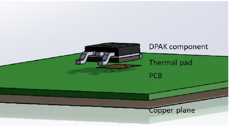
Figure 8: SolidWorks simulation setup [7]
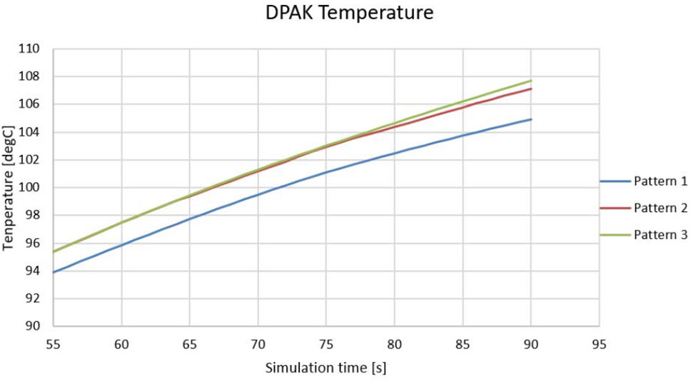
Figure 9: Thermal profile of DPAK with varying via patterns [7]
Based on the simulation results, pattern 1 emerges as the optimal via distribution. In this configuration, vias are evenly spaced beneath the DPAK component, allowing for effective heat dissipation over a wider surface area. Moreover, the same result has been verified practically in [7]. Though the difference in results (of pattern 1 to the others) are not extreme, they may be more significant at higher temperatures i.e., beyond 150 °C.
Thermal paste is another crucial component in the thermal management of electronics. It is also called heat sink compound, thermal compound, or thermal grease. When used with a heat-producing component, thermal pastes prevent the formation of air pockets that can render heat transfer (to the heat sink) ineffective, and enhances thermal conductivity ultimately making the PCB more rugged. Thermal pastes are of two types:
1. Silicone based
2. Silicone free
Silicone-based chemical formulations find extensive use in electronic applications, owing to their augmenting characteristics. Silicone possesses attributes that render it suitable for demanding operational environments, including resilience against vibration, chemicals, and wide temperature ranges. These formulations are typically composed of silicone polymers, like silicone oils or greases, blended with fillers to enhance thermal conductivity.
Silicone-free formulations are devoid of silicone compounds, relying instead on non-silicone polymers like acrylics, polyimides, or ceramics. Due to the absence of silicone, they demonstrate reduced outgassing tendencies, reducing the potential for contamination or deterioration of neighboring components.
The case study in [8] discusses effects of thermal aging on silicone-based and silicone-free thermal fillers. The results depict that post thermal aging at 125°C, the silicone-free material undergoes a hardening process, whereas the silicone-based material retains its viscoelastic properties. This suggests that the silicone-based material holds potential for prolonged use in high-temperature applications.
While silicone-based material exhibits superior mechanical and thermal attributes in high-temperature settings, the dielectric properties of silicone-free material reveal lower conductivity. This makes it a more suitable choice for applications requiring greater electrical insulation [8]. With 55 years of experience in electronics reworking products, Techspray offers Heat Sink Compounds – both silicone-based and silicon-free -- that are functional for temperature ranges of -55oC to 205oC and -40oC to 200oC.
Cleaning
Though mentioned at the end, thorough cleaning is the foremost critical step in ensuring long-term reliability and ruggedness of the PCB. Most documented PCB failures stem from contamination related to the manufacturing process that persists on the surface of the printed circuit board assembly (PCBA) following soldering operations, whether by hand, wave, or reflow methods. Thus, most of the faults can be avoided by merely cleaning the PCBA. In the context of climatic dependability, residues originating from reflow soldering are typically less concerning compared to the flux residues that persist post wave soldering. In the latter case, the residue is distributed across the entire surface of the PCBA, whereas in the former, the solder paste confines the residues to specific areas beneath and/or in the vicinity of SMT components [9].
Corrosion problems in electronics emerge because of the acidic residues. These residues, due to their hygroscopic properties, promote the water layer formation on PCBA surfaces under humid conditions. Even minor amounts of readily soluble acids can saturate the water film that forms in humid conditions, greatly increasing its conductivity. Residues with high water solubility tend to elevate leakage currents, resulting in potential corrosion of the PCBA. These effects escalate with rising temperatures [9].
Tin whiskers are tiny, spontaneous metal growths that can occur on the surface of tin-plated electronic components, potentially causing short circuits or malfunctions in electronic devices. One case study [10] compares tin whisker growth in cleaned and contaminated PCBAs. No whiskers are observed on the boards that utilize components cleaned prior to assembly, and followed by a post-assembly cleaning process, in line with high-reliability standards.
Whiskers are found in both the original, as-received assemblies, as well as the contaminated ones [10]. Figure 10 shows Images of SOIC20 components after 500 hours at 85°C/85% RH revealing the absence of whiskers in cases where components were cleaned before assembly and subjected to post-assembly cleaning procedures (a, b). Short whiskers were observed in as-received assemblies (c, d), while contaminated assemblies exhibited longer whiskers (e, f).
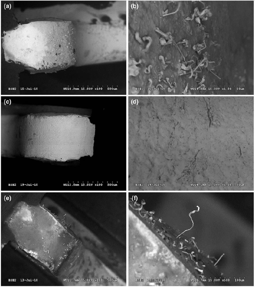
Figure 10: Tin whisker growth in cleaned vs contaminated PCBAs [10]
In conclusion, the article highlights some PCB ruggedization techniques crucial for enhancing durability and reliability in challenging environments. These methods, including conformal coating, potting, low pressure molding, edge-corner bonding, underfilling, cleaning, and EMI shielding, play a pivotal role in mitigating the impact of EMI, mechanical stress, temperature fluctuations, and moisture on PCB performance. By carefully selecting and implementing these techniques, electronics manufacturers can guarantee rugged electronic products.
Chemtronics & Techspray Products: Engineered to Enhance Reliability
Chemtronics and Techspray branded products offer a number of products to optimize device reliability and ruggedness. CircuitWorks Conductive Pens and Conductive Paint are convenient and effective ways to repair EMI shielding. For a comprehensive look at that process, check out our article “Using CircuitWorks Conductive Paint to Maximize High Frequency EMI/RF Shielding”
Techspray conformal coatings offer a wide range of resin types, including silicone, acrylic, and urethane. Fine-L-Kote SRV silicone coating passes stringent standards including MIL-STD 810G and MS941-04 salt spray tests, so it is ideal for moisture protection. If you are having trouble keeping a steady supply of Dowsil 1-2577, Fine-L-Kote SRV can be qualified as drop-in replacement.
Chemtronics has an expansive offering of Flux-Off flux removers, providing solutions no matter what type of flux is used. PFAS-free options are also available, for greater safety without performance trade-offs. Techspray offers a full line of replacements for 3M Novec Solvents, to keep your cleaning operation running through the Novec phase-out.
We are available to help qualify new cleaning processes, evaluate current processes, or troubleshoot contamination issues. For more information or technical support, contact Chemtronics at [email protected] or 678-928-5845.
References
[1] J. C. Y. C. J. L. Zhichao Wu, "Drop performance evaluation for application of different underfill processes," in 2017 18th International Conference on Electronic Packaging Technology (ICEPT), Harbin, China, 2017.
[2] S. Akbari, "Fracture of Underfilled and Edge-Bonded BGA-PCB Assemblies: Effects of Joint Geometry, Strain Rate and Stiffness," Semantic Scholar, 2017.
[3] J. C. Garrett Wong, "Dispensing EMI Shielding Materials: An Alternative to Sputtering," smtnet, 2019.
>[4] Z. L. N. H. Y. X. Y. Z. Y. C. Ligang Tan, "An investigation on shielding effectiveness of conductive adhesive," Microelectronics Reliability, vol. 106, 2020.
[5] B. T. M. T. T. N. D. Tang Tan Chien, "Improvement of shielding for electromagnetic compatibility," in 2016 International Conference on Electronics, Information, and Communications (ICEIC), Dannan, 2016.
[6] J. Keeping, "Conformal Coatings," in Lead‐free Soldering Process Development and Reliability, Wiley, 2020, pp. 429-465.
[7] R. J. G. C. D. P. A. Fodor, "Thermal Via Placement for High-Power applications," in 2017 IEEE 23rd International Symposium for Design and Technology in Electronic Packaging (SIITME), Constanta, 2017.
[8] M. M. R. M. K. P. P. D. R. B. R. R. D. A. A S M Raufur Chowdhury, "A Comparative Study of Thermal Aging Effect on the Properties of Silicone-Based and Silicone-Free Thermal Gap Filler Materials," Materials, vol. 14, no. 13, p. 20, 2021.
[9] F. L. R. A. Kamila Piotrowska, "Transformation of reflow solder flux residue under humid conditions," Microelectronics Reliability, vol. 123, p. 14, 2021.
[10] S. M. Z. B. E. K. M. R. &. J. K. Polina Snugovsky, "Whisker Formation Induced by Component and Assembly Ionic Contamination," Journal of Electronic Materials , vol. 41, no. 2, p. 204–223, 2012.
[11] LPMS-USA, "LPMS-USA," [Online]. Available: https://www.lpms-usa.com/services/low-pressure-molding/. [Accessed 20 09 2023].
Ask A Technical Question
Stay up-to-date on Chemtronics news, products, videos & more.