How to Identify and Solve Thermal Stress Issues in Solder Joints
Modern electronics assemblies are more often exposed to hard temperature conditions e.g., power supplies in airborne radars. Repeated thermal cycling induce thermal contractions and expansions in these electronics assemblies including the substrate of PCB, components and solder joints.
Rapid contractions and expansions may cause thermomechanical fatigue, which results in deformation of solder and subsequently degradation of solder joints. Thermomechanical fatigue is the major reason (55%) of failure in PCBA [1], as shown in figure 1.
In this article, based on the results of Finite Element Method (FEM), variations in dimensions of solder joints are discussed in order to reduce stress on BGA and improve reliability of solder joints, assuming realization of thermal power cycle.
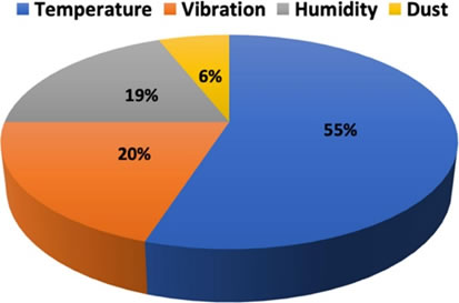
Figure 1: Causes of failure in PCBAs [2]
Threat of Thermal Stress on Reliability of Electronic Devices
In electronics, thermal cycling refers to the cycling of temperature between low and high values at a very rapid rate. The frequent temperature changes often result from power cycling, power dissipation or self-heating in electronic devices like MOSFETs, IGBTs and diodes or because of periodic change in environmental conditions.
Thermal cycling gives rise to stresses [3], which are induced because of mismatches in coefficient of thermal expansion (CTE). These stresses may cause creep deformationand evenplastic deformation in the solder joints at a melting point, which is the property of solder material. This mechanical degradation of solder is often termed as solder fatigue.
Excess solder fatigue can induce permanent cracks and fractures in solder joints as shown in figure 2. In electronics industry, particularly defense sector, for ensuring system reliability, and as part of PCB thermal management in post-development phase, electronics manufacturers procure dedicated temperature chambers to pass the PCB assemblies through thermal cycling. PCBs manufactured without considering effects of thermal cycling in design phase, tend to malfunction after thermal cycling. Fractured solder joints is the most common reason of PCBA malfunction.
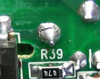
Figure 2: Fractured Solder joint [4]
Case Study: Thermal Stress in BGAs
Modern electronic manufacturing focus on electronics assemblies with minimum dimensions, form factor, and high component density. The surface mount technology (SMT) has attracted much attention in this regard, and the most compact IC package for SMT is the Ball Grid Array (BGA) as shown in figure 3. Today’s state of art electronic components mostly use BGA package e.g., Field Programmable Gate Arrays (FPGAs).
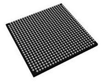
Figure 3: BGA Package [3]
A chip with BGA package (64 solder balls) is considered as case study. Radius of solder joint is 0.046 cm while the height of solder joint is 0.034 cm. Moreover, in this case study, solder material is selected as lead-free solder. For thermal loading, power density is varied from 2000000 W/m3 to 8000000 W/m3 with an interval of 10 minutes [1].
After 140 minutes of thermal power cycling, the results are presented in figure 4 and figure 5. It is evident that profiles of stress and strain are not constant, in fact those solder joints which are located at the edges experience greatest stress levels and strain levels and thus in a thermally stressed faulty PCBA, they might be the primary point of interest for the technicians or design engineers debugging the root cause of failure.
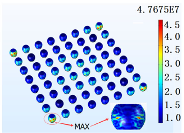
Figure 4: Stress (Pa) distribution of BGA package under thermal power cycling [1]
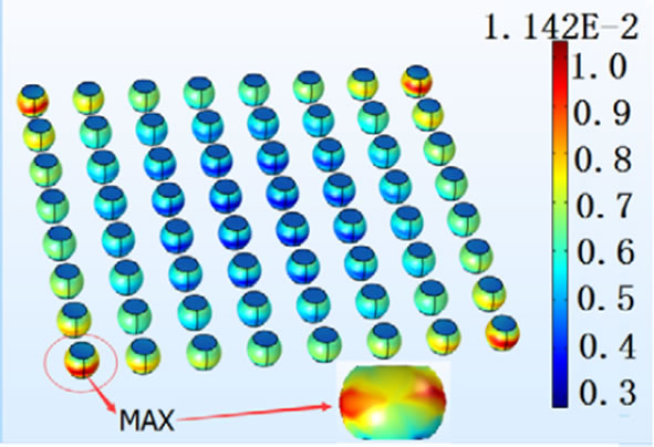
Figure 5: Strain distribution of BGA package under thermal power cycling [1]
For the technicians and the PCB design engineers, some best practices to avoid PCBA failures are presented next:
Increase Length of Solder Joint
To evaluate the effect of length of solder joints on stress and strain profiles in BGA package, experiments have suggested that increasing the length of BGA solder joint can decrease the peak stress and strain in solder joints making them less vulnerable to failure and increasing fatigue lifetime [1]. When length of solder joint is increased, the resistance offered to solder expansion also increases. The energy of deformation reduces and resultantly stress reduces as well. For further analysis, the results are summarized in Table 1.
|
Solder Joint Height (cm) |
0.03 |
0.032 |
0.034 |
0.036 |
0.038 |
|
Stress Level (MPa) |
71.785 |
68.379 |
47.675 |
40.785 |
38.375 |
|
Strain (unit less) |
12.1 |
10.4 |
11.4 |
10.5 |
9.9 |
Table 1: Variation of stress-strain profile with solder joint's height
Reduce Diameter of Solder Joint
Keeping the length of solder joint constant, the effect of varying BGA solder joint’s diameter is presented. Based on FEM, reducing diameter of BGA solder joint may decrease maximum thermal stress and strain [1], as described in Table 2.
|
Solder Joint Diameter (cm) |
0.042 |
0.044 |
0.046 |
0.048 |
0.05 |
|
Stress Level (MPa) |
40.172 |
43.364 |
47.675 |
50.938 |
59.057 |
|
Strain (unit less) |
11.1 |
11.2 |
11.4 |
11.5 |
12.6 |
Table 2: Variation of stress-strain profile with solder joint's diameter
Use Softer Solder Material
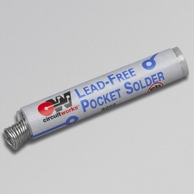
Hard solder materials i.e. with high modulus (gold-tin alloy) may cause increased thermal stresses in BGA solder joints as compared to soft solder materials i.e. with low modulus (silver-tin). CircuitWorks Lead-free Solder (part # S200) is made from lead-free solder alloy SAC 305 and it is capable to provide reliable solder connections. Electronics industry is now shifting to SnAgCu (SAC) solder alloys. In a recent study [2], four lead-free SAC alloys, SAC305, SAC387, SAC396 and SAC405 are compared with the corresponding stress and strain values after 6 cycles of thermal cycling. This is shown in figure 6and figure 7.
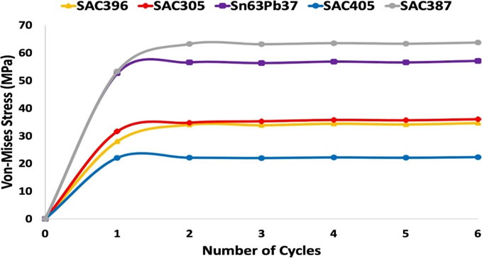
Figure 6: Stress comparison in different lead-free solder materials after thermal cycling [2]

Figure 7: Strain comparison in different lead-free solder materials after thermal cycling [2]
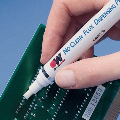
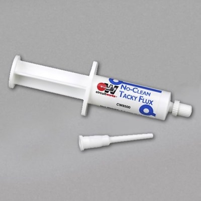
The SAC405 solder joints were found to possess the greatest thermal fatigue life and hence experience lowest stress and strain. CircuitWorks Tacky Flux (part # CW8700) specifically designed for BGA rework requirements of higher temperature and Lead-free applications, is a popular choice for such tasks. Its high viscosity allows easy application, and it will not leave behind any ionic residue that can negatively impact PCBA reliability.
Use More Copper in Vias
Copper being a ductile material can withstand many cycles of contractions and expansions. Increasing amount of copper in vias can greatly improve thermal cycling reliability. A via with 0.15 cm diameter and copper thickness of 44.4 cm3 of plating is mechanically strong enough to prevent appearance of cracks.
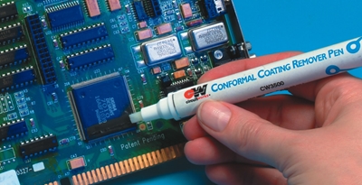
Apply Conformal Coating
Conformal coating is a very thin layer of insulating material applied to PCBAs to protect them from rough environments. Typical thickness of conformal coatings range from 1 to 5 mils. These coatings are useful to reduce thermal stresses in mission critical applications. Conformal coatings are of following types:
- Silicone (SR)
- Acrylic (AR)
- Epoxy (ER)
- Parylene (XY)
- Polyurethane (UR)
While selecting a suitable material for conformal coating, the properties of PCBA assembly particularly CTE must be considered. Coating thickness is another deciding factor. Thicker coatings are most likely to fail in a BGA package [5].
Since conformal coating can penetrate beneath BGA package, it directly influences strength of solder joints. Suitable coating material, if properly applied, can strengthen the solder joints and reduce solder fatigue. If not properly applied or using inappropriate materials i.e., those having CTE greatly different from that of PCB, can further increase solder joint fatigue.
For example, most Pb-free solders have a CTE of less than 25 ppm/oC and acrylic conformal coatings generally have CTE around 70 ppm/oC [5]. Solder joints on this coated PCBA suffer from solder fatigue due to mechanical stresses generated due to thermal or power cycling.
To prevent conformal coating from adding to the physical stresses impacting BGA solder joints, it is common to mask off, or otherwise prevent the application of conformal coating over and around BGAs. 2-3 mm keep-out area around a low stand-off component is recommended to avoid the material from being drawn under by wicking action.
Selective spray equipment can be used for accurate application of the conformal coating around low stand-off BGA components. A very high viscosity conformal coating “dam” can also be applied around the keep-out area to prevent the lower viscosity material from flowing too close to the BGA.
Conformal coating is also engineered to withstand thermal cycling without breaking down. The relevant standard to test conformal coating under thermal stress is IPC-TM-650, method 2.6.7.1., which is included in the overall conformal coating qualification standard IPC-CC-830. This test cycles a test board between -65°C (-85°F) and 125°C (257°F) for 100 cycles. Then the temperature and humidity are allowed to stabilize to 25 ±5°C (77 ± 9°F) and relative humidity of 50 ±5%. After 24 hours, the coating appearance is visually evaluated and tested for dielectric withstanding voltage.
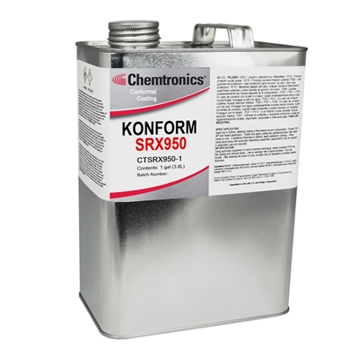
Chemtronics Konform® SR-X Silicone Conformal Coating
Chemtronics Konform brand provides wide range of conformal coatings including Konform SRX Silicone Conformal coating. Konform SR-X provides maximum flexibility and protection from extreme temperatures, harsh environments, and vibration damage.
Konform SR-X is a one-part, clear conformal coating with moisture, corrosion and abrasion resistance. It was developed to be the best alternative for Dow Corning conformal coating 1-2577 and 1-2620.
This high-gloss transparent conformal coating provides ideal protection for both rigid and flexible printed circuit boards. Cured coatings are hydrolytically stable and retain their physical electrical properties after high temperature and humidity exposure.
Like all Chemtronics Konform coatings, Konform SR-X is IPC-CC-830B certified.
Conclusion
In this article, one of the most common causes of failure in electronics assemblies is discussed with focus on BGA package. Fracture in solder joints due to thermal fatigue is a potential cause of PCBA failure. To reduce chances of failure, length of solder joint must increase and diameter of solder joints must decrease. Using soft solder materials and using more copper in vias, strong solder joints can be formed. Moreover, if proper material selection is made, conformal coating can be an effective technique to decrease solder fatigue.
For more information on CircuitWorks rework, repair and prototype products, and Konform conformal coatings, contact an application specialist at [email protected] or 770-424-4888.
References:
[2] S. M. E. H. Joshua A. Depiver, "Thermal fatigue life of ball grid array (BGA) solder joints made from different alloy compositions," Engineering Failure Analysis, vol. 125, 2021.
[3] Digikey. [Online]. Available: https://www.digikey.ee/en/products/detail/xilinx-inc/XC7S25-1CSGA225C/8040779.
[4] "Siber-sonic," Siber-sonic, 9 January 2021. [Online]. Available: https://siber-sonic.com/electronics/fracturedSJ.html. [Accessed 2021].
[5] C. M. K. S. D. S. G. P. Abid-Alrahman Fawzi Abbas, "Impact of Conformal Coating Material on the Long-Term Reliability of Ball Grid Array Solder Joints," Procedia Manufacturing, vol. 38, pp. 1138-1142, 2019.
Ask A Technical Question
Stay up-to-date on Chemtronics news, products, videos & more.
Related Products